Base module “Orion” is intended for using in enterprises and organizations dealing with oil, gas and geological exploration, in organizations dealing with complex systems engineering and design, in commercial organizations of scientific and technical area and high tech, and for solving various applied tasks such as:
- remote sensing and tomography;
- monitoring systems design;
- simulation of complex technical and natural objects and processes;
- design of information control systems for real time control of complex objects;
- design of microelectronic products.
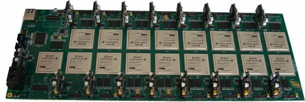
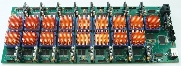
Base module “Orion” consists of:
- controller of computation module board designed on the base of FPGA Xilinx XC5VLX50T-1FF1136C;
- computation field composed of 16 FPGA Xilinx XC5VLX110-1FFG1153 Virtex 5. FPGAs of computation field are connected into a ring. Connection between neighbouring FPGAs is provided by differential lines of LVDS-interface on a frequency of 1200 MHz;
- nodes of basic (X5 and chip DD26 Xilinx XCF32PV048C) and reserve FPGA loading via JTAG interface (X7);
- subsystem of synchronization (generators DD19, DD20 ECS-2033-250-BN of ECS INC International and clock pulses distributors IDT5T9316NLI of Integrated Device Technology, Inc.);
- distributed memory composed of 32 chips of dynamic memory (MT47H64M16HR-25E of Micron Technology, Inc., 64 М*16 and write/read frequency up to 400 MHz). Two memory chips DDR2 are connected to FPGA DD2-DD16 of computation field and to FPGA of base module controller DD17. RAM memory space is 4 GBytes;
- 2 channels of LVDS interface composed of 14 differential pairs (connectors X2 and X3: QTE-014-01-L-D-DP-A-K) for connection with input/output unit (connection with personal computer) and external devices;
- subsystem of FPGA loading;
- power subsystem composed of DC-DC transducers (portable voltage transducers), generating power supply voltage;
+1 V – power of FPGA cores;
+2.5 V – power of FPGA buffer stages, memory and clock node;
+3.3 V – power of clock node.
Technical Specifications
- FPGA XC5VLX110-1FFG1153 (computation FPGA)
(11 million of equivalent gates in each FPGA) - 16
- FPGA XC5VLX50T-1FFG1136 (controller of the base module)
(5 million of equivalent gates in each FPGA) - 1
- Memory chips DDR2 MT47H64M16HR-25E (64 М * 16 = 1024 М) – 32
- Memory size, GByte - 4
- FPGA frequency, MHz - 300-330
- Clock rate of differential lines between neighboring FPGAs and between FPGAs and connectors, MHz – up to 1200
- Performance, GFlops - 200
- Interface Ethernet, GBit/sec - 1
- Interface LVDS channels, pairs (connection of base module with personal computer via PCI-E) - 14
- Connectors SS4 (Samtec), (data LVDS channels) - 6
- LVDS channels for data exchange with neighbouring devices, pairs - 133
- Power consumption, less than, W - 250
- Dimensions of BM, mm - 154*412
- Cost, rubles - 1 300 000